
Electronic assemblies without PCBs – Electronic Products & TechnologyElectronic Products & Technology
Laser immediate structuring (LDS) is a special good results tale. For pretty much 20 several years, it has been attainable to utilize electronic conductor paths right onto plastic pieces throughout sequence output. LDS permits the generation of electronic assemblies with versatile geometric shapes. This procedure enables digital products (these as sensible phones, sensors or health care products) to turn into even more compact and more strong. Automated manufacturing procedures also make this method extra economically appealing.
There is significantly less and significantly less area available for digital assemblies, so solutions are necessary which substitute standard printed circuit boards. LDS allows further miniaturization and makes ever more complicated geometric styles possible. This is a stable and trusted approach that has recognized itself in high-quality-vital sectors these kinds of as health-related technologies or safety-applicable components for the automotive business.
LDS process enables a few-dimensional assemblies
Direct laser structuring enables 3D-MID (Mechatronic Integrated Gadgets) assemblies to be produced. When working with 3D-MID, electronic factors can be equipped instantly onto a a few-dimensional base physique, without circuit boards or connecting cables. The base system is created applying an injection moulding procedure, whereby the thermoplastic materials has a non-conductive, inorganic additive.
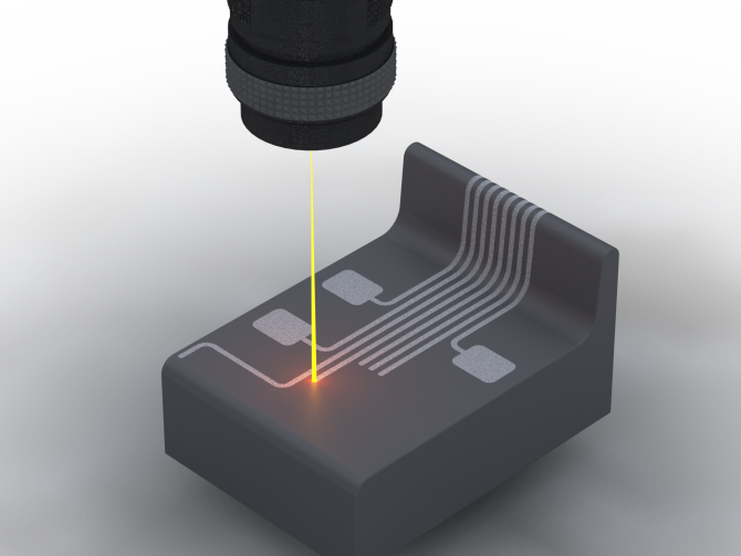
The structure of the conductor path is utilized employing the LDS system.
LDS allows electronic assemblies to be created in adaptable geometric shapes. Sensible phones, listening to aids and wise watches are turning into lesser and more strong many thanks to this procedure. Source: Harting
The additives in the product are “activated” by immediate laser structuring so that the plastic substance can accommodate the electrical conductor paths. The laser beam writes the areas supposed for the conductor paths and produces a micro-rough framework. The unveiled steel particles sort the nuclei for the subsequent chemical metallisation. In this way, the electrical conductor paths are utilized to the parts marked by the laser. The other places of the three-dimensional base physique keep on being unchanged. The plastic ingredient can then be assembled in standard SMD processes comparable to a standard PCB. It is also suited for soldering in a reflow oven.
Multipurpose software of laser technological know-how
As one of the greatest suppliers of 3D-MID factors outside the house of Asia, HARTING utilizes substantial-effectiveness laser systems for the LDS method, with three lasers performing in parallel, every offset by 45 levels. Many thanks to an additional axis of rotation, parts can be processed by the laser simultaneously from all sides (360 degrees). This technological know-how allows versatile geometric designs, this kind of as reflector shells or LED lights, to be created. Inspite of the small conductor route thickness of 16 to 20 μm, the conductor paths are nevertheless suited for demanding automotive elements or for applications with currents up to 10 A – for instance for heating coils in cameras which are employed to prevent the optics from fogging up
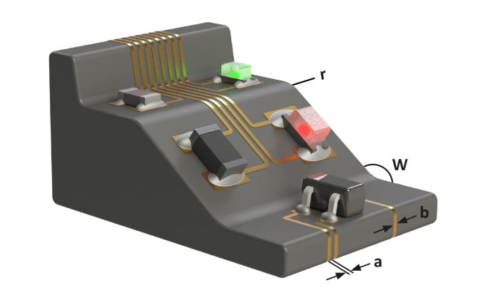
Minimum distances involving the conductor paths (a): 50 – 150μm. Minimum amount width of the conductor paths (b): 50 – 150μm Radius (r): .2mm. Source: Harting
Regular alterations for the duration of the electronics enhancement period or new factors with modified dimensions can lead to highly-priced changes during traditional PCB generation. The laser structure, in distinction, can be tailored quite flexibly by making use of the parameters of the laser’s regulate application. No adjustments in the injection moulding are demanded for this.
The production of prototypes applying LDS is also less difficult compared to conventional procedures. HARTING can produce the plastic base entire body using LDS-compatible material and 3D printing. Injection moulding can also be used with inexpensive prototype instruments.
New tendencies in the LDS procedure
Various aspects of LDS know-how have been improved and further more designed around the earlier several yrs.
- The operating area of the laser has been enlarged from 160 x 160 x 80 mm to 200 mm x 200 mm x 80 mm, thus enabling a increased packing density and the processing of even larger sized parts.
- The performing pace of the laser can be doubled to 4 m/s by optimizing the servo models and mirrors which guidebook the laser beam, thus considerably minimizing the processing time.
- The enhancement of the optics allows the use of a laser with a diameter of 100 μm and a laser with a good emphasis of 50 μm for processing even more compact structures.
HARTING is the only 3D-MID company in the earth that has a laser technique with three fine aim optics of 50 μm. Even more compact conductor path gaps can be achieved thanks to this wonderful aim laser. Therefore, quite a few conductor paths can be produced on the similar element and a better packing density can be executed. This is utilised for safety engineering, between other items, simply because the closely spaced and intertwined conductors are capable of triggering protection alarms from even the smallest bodily interference.
Advancements in components and economics
Only specifically selected thermoplastics are certified for the LDS approach these are readily available from stock. The process can be more enhanced with shopper-particular changes to the plastic substance:
- HARTING works by using a system which adds LDS additives to non-accredited materials to make them MID-appropriate.
- Certain RAL or Pantone colors can be reached with MID plastics by using colour pigments and unique LDS additives.
- By selecting suited additives, particular RF properties can also be carried out, depending on the frequency variety.

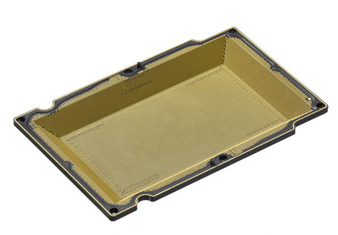
Digital parts – such as LEDs, ICs, photodiodes and sensors – can be attached directly onto the part carrier. The assembled part carriers can then be processed as typical SMD components. Source: Harting
To additional enhance the price-performance of the producing system, HARTING relies on automated robotic methods. The LDS laser technique is geared up with a rotary indexing table so that a part can be inserted or taken out when a different component is nonetheless becoming processed. The in-feed and unloading methods are automatic by HARTING making use of robotics. This improves throughput and autonomy, even though also enabling integration into automatic manufacturing procedures. An extra automation move is delivered through the injection moulding course of action. Below, as well, a robot will take about the removing of the injection moulded sections. The use of robotics also enhances the exact reproducibility of the procedures and, as a result, all round item excellent.
Far more advancement for 3D-MID
The 3D-MID caps defend the electronics from unauthorized accessibility both equally mechanically and electronically. A extremely specific meandering structure detects every single accessibility, no make any difference how little, and for that reason helps prevent theft. Resource: Harting
HARTING studies amplified demand for MID initiatives and has even more expanded the 3D-MID division by investing in equipment and by attaining a competitor’s small business. Revolutionary in-residence merchandise are also contributing to further more growth. HARTING has created a solution dependent on 3D-MID know-how which replaces versatile PCBs with a element carrier. Alternatively of using a flex-PCB, the element provider can be fitted directly with digital elements, consequently saving up to two thirds of the charge.
—————————————-
About HARTING 3D-MID
HARTING 3D-MID is giving the full price chain for 3D-MID systems from a single source, including improvement/prototyping of client-unique products and solutions, injection moulding, laser direct structuring, metallization, assembly and relationship technological innovation, as effectively as ultimate inspection. Its core organization is the creation of mechatronic parts for auto manufacturing, market, clinical technological know-how and sensor devices.
Dirk Rettschlag, venture manager & IE MID at Harting MID.